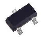
VDS= 20V
RDS(ON), Vgs@-2.5V, Ids@
RDS(ON), Vgs@4.5V, Ids@
Features
Advanced trench process technology
High Density Cell Design For Ultra Low On-Resistance
SOT-23 Internal Schematic Diagram
Top View N-Channel MOSFET
Maximum Ratings and Thermal Characteristics (TA=
Parameter | Symbol | Limit | Unit | |
Drain-Source Voltage | VDS | 20 | V | |
Gate-Source Voltage | VGS | ±8 | ||
Continuous Drain Current | ID | 2.3 | A | |
Pulsed Drain Current 1) | IDM | 8 | ||
Maximum Power Dissipation | TA= | PD | 1.25 | W |
TA= | 0.8 | |||
Operating Junction and Storage Temperature Range | TJ, Tstg | -55 to 150 | ℃ | |
Junction-to-Ambient Thermal Resistance (PCB mounted)2) | RθJA | 140 | ℃/W | |
Note: 1. Repetitive Rating: Pulse width limited by the maximum junction temperature
2. 1-in2
Electrical Characteristics
Parameter | Symbol | Test Condition | Min | Typ | Max | Unit |
Static | ||||||
Drain-Source Breakdown Voltage | BVDSS | VGS = 0V, ID = 250uA | 20 | -- | -- | V |
Drain-Source On-Stage Resistance | RDS(on) | VGS = 4.5V, ID = | -- | 40.0 | 60.0 | mΩ |
Drain-Source On-Stage Resistance | RDS(on) | VGS = 2.5V, ID = | -- | 50.0 | 115.0 | |
Drain-Source On-Stage Resistance | RDS(on) | VGS = 1.8V, ID = | -- | 80.0 | 130.0 | |
Gate Threshold Voltage | VGS(th) | VDS = VGS, ID = 250uA | 0.6 | -- | 1.2 | V |
Zero Gate Voltage Drain Current | IDSS | VDS = 20V, VGS = 0V | -- | -- | 1 | uA |
Gate Body Leakage | IGSS | VGS = ±8V, IDS=0uA | -- | -- | ±100 | nA |
Dynamic3) | ||||||
Total Gate Charge | Qg | VDS = 10V, ID = VGS = 4.5V | -- | 4.5 | 5.85 | nC |
| ||||||
 已验证
已验证


